Accelerator, Laser, and Coherent Optoelectronics R&D Lab (ALCOL)
Cathode Study
-
Development of Ultra-Short Electron Beam Source
For the plan to develop a short pulse electron beam source construction for an UEDM system, a 5.5 MW S-band klystron (Thales TH2163) and modulator (ScandiNova K1 turnkey system) were installed and commissioned at FW110 in collaborating with ScandiNova. The startup test ended up successfully demonstrating ~ 5.2 MW with 4 ms pulse width. We documented safety issues of the high energy electron source and the management plan, which was reviewed by the campus radiation safety officer (RSO) and campus safety committee for several months. After the review, the construction plan of the ultra-short pulse electron source and linear accelerator system was fully approved and the purchase order of a single-gap RF-gun was placed as a first step of the endeavor. A single-gap electron gun (0.5 – 1 MeV) was designed in the collaboration with Far-Tech, including the beam dynamics analysis by computer simulations. The gun has been built and it is scheduled to be delivered to NIU within a month. During the time, we designed the beam diagnostics setup to test the RF-gun, which consists of beam-focusing magnet, Faraday cup, image station, steering magnet, etc. Most recently, a DOE (BES) STTR proposal titled the “Time-stabilized ultrafast electron diffraction and microscopy” has been awarded on the ultra-short electron source. In the scope of project, we plan to reach out to the community to search for potential users of a facility that would be built at NIU in Phase II and assess the science that can be done at this facility in order to refine the requirements for the electron and laser beam parameters and their relative stability. We will also develop the concept of the detector system and CCD camera, including the fluorescent screen material and the choice of CCD camera, method of steering the particle beam away from the CCD camera, a rough CAD model of the sub-system, and price quotes for the major components.
Abstract
Electron beams emitted from a cold cathode are thermally stable and mono-energetic with a small phase-space volume. We have been developing a field-emission type RF-gun system for high brightness electron source applications, including electron scattering/diffraction and tunable coherent X-ray/THz generation. The system consists of a single-gap gun-cavity and an S-band klystron/modulator capable of powering the gun with up to 5.5 MW peak (PRR = 1 Hz, duration = 2.5 ms). The designed gun built with the symmetrised side-couplers has surface field on the cathode ranging 50 – 100 MV/m with 1.3 – 1.7 MW klystron-power and 1.2 field ratio (HFSS). ASTRA simulations also indicate that the gun produces the beam with transverse emittances of less than 1 mm-mrad with 10 – 20 pC bunch charge at 500 keV beam energy. Under the gun operating condition, particle tracking/PIC simulations (CST) show that a single-tip CNT field-emitter produces short pulsed bunches (~ 1/10 RF-cycle) with small emittance (£ 0.01 mm-mrad) and high peak current density (³ 10,000 kA/cm2). After the gun is fully installed and commissioned, a CNT-tip cathode will be tested with RF-field emission.
Introduction
Beam brightness cannot be improved, but only spoiled along the downstream accelerator. Therefore, high quantum efficiency (QE) and low intrinsic emittance, plus long lifetime, are very necessary for injector-type electron sources. The beam emitters of the electron sources are required to have a high QE and uniform emission at the longest possible wavelength with fast response time (< 100 ps). Emittance can be diluted by space charge expansion seeded by non-uniform electron emission. In order to minimize intrinsic emittance, cathode surfaces should preferably be atomically flat within a few nanometers of peak-to-peak variation. Furthermore, operating lifetime of more than 1 year with a reasonable vacuum level of 10-10 Torr range and easy, reliable cathode cleaning or rejuvenation/re-activation is strongly preferred.
Linac-based coherent radiation sources need bright electron beams, but injectors comprised of conventional DC-guns and RF-bunchers for longitudinal pulse compression have inherent limitations in reducing transverse and longitudinal emittance. While thermionic and photo-cathodes have been most widely employed with injectors for accelerator machines, certainly there are some practical limits in applying them to a compact, high brightness electron source [1 – 4].
Usually, field emitters have been studied for the applications of long pulse operation. The main advantages of field emission are that it simply generates pulsed beam and that the beams emitted under the emitters have low transverse emittance. Normally, the thermionic cathodes and field emitters are tolerant of poor vacuum and they have a long operating lifetime. However, the beam from the electron sources usually has long a bunch length (> 100 ps) and large longitudinal emittance with a lack of beam-profile control. Although high beam currents could be created and accelerated by an electron gun with field-emitters, it is difficult to find stable and reproducible operating conditions. Recently, various cathode materials have been extensively developed for vacuum microelectronic applications [5]. While actual RF devices like field-emitter tube amplifiers are still based on tip arrays of refractory metals, cathodes with nano-crystalline diamond materials would be preferred, if the field emitters have sufficient uniformity and high current stability.
CNT-tip field-emitter cathode
Flat panel display technology with commercial interest has stimulated research on the fabrication and characterization of nanostructured materials for field emission applications. However, it turned out that low cost fabrication over large areas is very challenging, particularly for applications demanding large emission currents requiring robust emitter materials. It was found that CNTs are quite suitable for the application as they are low-cost, robust, nano-structured material [6]. Previously, field emission of CNT cathodes was demonstrated with multi-walled carbon nanotubes (MWNTs) as well as single-walled carbon nanotubes (SWNTs) [7]. Carbon nanotubes have several advantages over other field-emitting materials. In contrast to commonly used emitters such as tungsten, a nanotube is not a metal, but a structure built by covalent bonds. The activation energy for surface migration of the emitter atoms is thus much larger than for a tungsten electron source. Therefore, the tip can withstand extremely strong fields (several V/nm). Depending on the exact arrangement of the carbon atoms, the cylinders are semiconducting or metallic conductors and the tubes can be closed or open at one or both ends. Furthermore, when compared with other film field emitters such as diamond or amorphous carbon structures, CNTs show a high aspect ratio, a small radius of curvature of the cap and good conductance [8]. The small diameter of CNTs (diameter of a single SWNT can be - 1 nm) enables efficient emission at low fields, despite their relatively high work function (> 4.5eV). At 1 – 3 V/pm of emission threshold fields, CNTs are most suited for low-power, high-current density applications and are more robust than diamond, with the ability to deliver current densities in excess of 1 A/cm2. Some prior work reported that a single CNT is capable of emitting 30 nA, so achievable current densities with CNTs might be orders of magnitude higher. The emitted current from a field emitter depends directly upon the local electric field at the emitting surface determined by very small variations in the emitter geometry and surface conditions. The main variables of emission performance with respect to the amount of electron current are alignment, purification, end type (open or closed), density and spacing of tubes. Remarkable progress has been made on high current emission of the CNT emitters for electron beam devices, but much more work is still needed to achieve the level of uniformity, brightness, and stability required for injector and accelerator application.
The Fowler-Nordheim equation represents the emission current density on the flat cathode in one-dimensional space. However, FE tips, especially CNTs, have much more complicated physical shapes, so the presence of a CNT tip on the flat geometry can significantly distort the electrical field distribution around the tip area. The spatial field variation allows different sites on the tip to experience different electric fields. Considering the tip geometry and actual field distribution in the vicinity of the tip end, one can see that an accurate evaluation of the emission current of a CNT according to the applied voltage is a critical issue that has been long studied. The possible irregularities of spatial field distributions and geometrical shapes of CNTs resulting from uniformity of arrayed tips, emission characteristics relying on absorbed molecules, and uncontrollable distribution of electronic properties set up unknown factors on the CNT emission characteristics, which are not properly represented in the Fowler-Nordheim equation.
The ratio of field distortion due to the presence of a charged object(s) in the space is parameterized by the electric field enhancement factor b = E/E0, where E0 (= U/L) is the electric field between the electrodes (U and L: the anode-cathode voltage and distance, respectively). For theoretical analysis, the local electric field, E, was approximated by various analytic forms (e.g. b » r(1 + d/D), where D is the tip-to-tip distance) of the field enhancement factor, b. In principle, as the aspect ratio (r = l/d) of CNTs exceeds 1000, field emission from nanotubes would occur at a much lower voltage applied than conventional field emitters. Typical computer simulation based on electrostatic finite element algorithms can provide very accurate solutions of the local field distribution, E, which is directly implemented in FN equation (Fig. 1). The transverse emittances and intrinsic energy spread of the electron bunch emitted from a cathode are mostly determined by initial beam conditions, when electrons are created at a cathode surface. Although the electron beam emitted from CNT tips has a small transverse emittance, the emission condition of CNTs is strongly dependent upon the field enhancement factor, which sensitively varies with the shape of the nanotube tip.
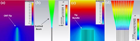
Figure 1: Electrostatic potential distributions, (a) and (c), and beam energy distributions,(b) and (d), of single-tip and CNT tip array.

Figure 2: Beam emission simulations of single-tip CNT models (a) closed CNT-tip and its (b) hemisphere model, and (c) open CNT-tip and its (d) cylinder- and (e) hollow-model (f) J-V plot at the tip-ends (g) transverse emittance and (h) beam envelop versus distance from the tip end under 70 V/mm field.
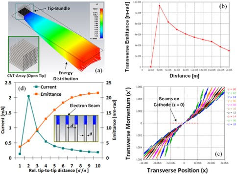
Figure 3: Field-emission model (tracking solver) of CNT tip array (1 ´ 1 mm2) (a) spatial energy distribution of emitted beam (b) transverse emittance versus distance (c) x-x¢ plots with distances (d) emission current and beam emittance versus tip-to-tip distance (d) normalized by tube diameter (a).
Nanotube tips, CVD-grown on a catalyst seed, normally have hemi-spherically closed ends, as shown in Figs. 2(a). The spherical structure of the CNT tip surface increases beam divergence. With the large transverse momentum, there might be a limit to the reduction of the beam emittance and intrinsic energy spread. The open structure (Fig. 2(c)) is more effective in increasing emission current density and reducing energy spread. The field-emission simulation results (Figs. 2 (f – h)) with f = 4.5 eV on a 100 nm wide and 2 mm long CNT tip indicate that the open tip, in particular the hollow tip structure, has a much higher emission current density and smaller transverse emittance and beam envelope due to the flat surface of the emitting area and the smaller space charge effect. The emission area modeled with 1 ´ 1 mm2 generates the beam in a small envelope with sub-micron emittance (Fig. 3). As shown in Fig. 3 (c), although the phase-spaces of individual beams from the CNT tips are uncorrelated to each other at the initial emission time, the beam-to-beam correlation occurs as the beam evolves in time. The simulation result verified that the CNT tip array could be designed for exceptionally large emission current and small beam emittance by optimizing the field enhancement factor of multiple tips, in particular tip-to-tip distance (Fig. 3(d)). The simulation predicts that CNT tips have about two orders of magnitude lower field-threshold than other field emission cathode materials typically used. The chemical vapor deposition (CVD) process is capable of producing highly ordered vertically aligned CNT tip arrays. We have been collaborating with a commercial company on the idea to develop CVD-grown, free-standing multi-wall and single-wall CNTs, including CNT composites, ranging 5 – 20 mm in length and 10 – 30 nm in diameter in industrial and research grades. Our plan is to fabricate a cathode with vertically aligned, free-standing CNT tips with the CVD process, which are ~ 10 mm long, and to optimize process conditions and CNT dimensions.
RF-gun system for cathode tests
We have been constructing a RF-gun system for multiple types of cathode emission/lifetime tests, as shown in Fig. 4. The system consists of an S-band klystron (2.856 GHz) and power supply/modulator powering a RF gun. The klystron is capable of providing 5.5 MW peak power to a RF gun over 2.5 ms. This pulse driver is sufficiently powerful to impose extremely high RF-field on a cathode surface beyond the CNT emission field threshold, ranging from a few tens V/mm, which can readily liberate electrons from CNT tips. The RF-gun design is thus based on a single-cavity resonator operating in TM010 accelerating-mode, here with the cathode in the center of the cavity [74, 75], as shown in Fig. 4(c). We completed a vacuum leak test indicating that the gun has no leak under a UHV of 10-9 Torr level. Also, the gun was test by an HP 8720ES network analyzer, as shown in Fig. 4(d). The RF-test using a circle fitting program showed that the gun has a resonance frequency of 2.8555 GHz (TM010 mode) with Ohmic Q (Q0) = 7714, external Q (Qexe) = 7445, and loaded Q (QL) = 3788. We were aiming for a frequency target of 2.85551, which would result in a resonance frequency of 2.856000 when the device is put under vacuum and the temperature is raised to 34 °C. The tuning target takes account of the dielectric constant of air at 25C and 40% relative humidity and the temperature differences between the measured and as-installed environment. The final resonance frequency value of 2.855496 GHz corresponds to the gun being in tune under vacuum at a temperature of 33.6 °C. The coupling of the sample loop was tested with the network analyzer un-calibrated, since it is difficult to make a calibration with two dis-similar ports (waveguide and co-axial). The coupling is approximately -69 dB, which is close to the target -70 dB of coupling. This would result in a 20 dBm signal for a 1 MW on frequency input into the waveguide. The coupling was tested without compressing the vacuum gasket, which would lead to about 3 – 5 dB stronger coupling. The sample loop can also be rotated in order to decrease the coupling according to a cosine relationship if it is desirable to have less coupling. In the cathode plug, a cathode substrate will be glued to a removable copper socket of 8 mm diameter with a vacuum-stable and well-conducting silver lacquer. The cathode will be thermally stabilized by a special cooling circuit in the Cu socket.
Figure 4: NIU RF-gun system for cathode tests (a) outline of RF-injector system (b) photo of S-band klystron system under commissioning (c) electron gun assembled with a RF-window for vacuum leak test (d) measured signal transmission/reflection data of the gun: real/imaginary (L) and S11 spectrum (R).
CONCLUSION
A high brightness electron source with field emission type cathodes has been developed for generation of relativistic electron bunches with high current and low emittance from a carbon nanotube (CNT) emitter array. The S-band RF-gun is currently being constructed and we will test CNT emitter arrays with the field-emission mode, once construction is complete.
acknowledgment
We thank M. Figora, G. Fagerberg for the technical support and P. R. G. Piot of Northern Illinois University for the helpful discussion for system construction.
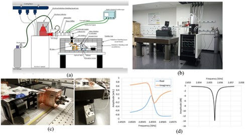
Figure 4: NIU RF-gun system for cathode tests (a) outline of RF-injector system (b) photo of S-band klystron system under commissioning (c) electron gun assembled with a RF-window for vacuum leak test (d) measured signal transmission/reflection data of the gun: real/imaginary (L) and S11 spectrum (R).

Table: Cathode Material versus Threshold Field